GPS-Locked 9cm Transverter
4 minute read
August 2007
When I built my GPS-Locked 10MHz reference oscillator it was always my intention to then use it as the reference source for phase-locking the local oscillators in my microwave transverters. The practice of GPS-Locking transverter LOs is often spoken of as the ‘holy-grail’ in terms of oscillator stability and accuracy, and one could be forgiven for thinking that implementing this kind of frequency control is expensive and complicated. The truth is that nowadays it is less complicated and less expensive than ever before thanks to the availability of GPS receivers and oven-controlled reference oscillators on Ebay. But how does one then go about locking a 135.666666MHz oscillator to 10MHz? Luis Cupido, CT1DMK, has been phase-locking local oscillators for a number of years now and along with Darrell Ward, VE1ALQ, has developed a versatile PLL board which can be used to lock almost any local oscillator (within reason) to 10MHz. The principle is simply this, divide both the LO and Reference frequencies by separate integers such that the same number is achieved. This is where the clever stuff comes in. Darrell and Luis’ board employs a CPLD (CMOS EEPROM-based Programmable Logic Device) which is programmed to incorporate the two configurable divide chains. The output is an Exclusive-OR gate which drives a simple R-C network, producing a DC voltage. This voltage is then tailored to drive whatever varactor is employed to tune the Local Oscillator.
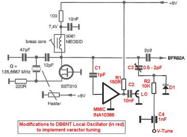
The circuit diagram on the right shows the modifications made by myself to my DB6NT 9cm transverter. All the components annotated in red were either ‘in-stock’ or found in the junk box! C3 is a green ‘Sky’ trimmer which is unfortunately no longer manufactured, but any high-quality trimmer capacitor offering a similar range can be used. To be honest, I have no idea what the varicap diode (D1) is other than it was supplied by Cirkit (sadly no longer in business) and is therefore probably a BB109. However anything similar to an MMBV809L is to be recommended. Because of the nature of this oscillator design, in order to ‘tap off’ some RF for the PLL board, it was necessary to include the INA10386 MMIC in order to provide sufficient buffering and minimum capacitive loading. A MAR-3 can be used as an alternative to the INA10386. I found the output of the MMIC to be +1dBm at 135MHz, which is more than adequate to drive the RF input on the PLL board.
135MHz Output
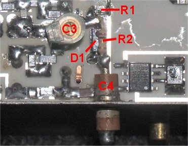
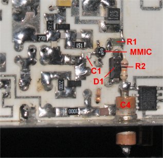
Just a photograph to show the placement of C3 in the scheme of things ...
Obvious, really.
Finally ...
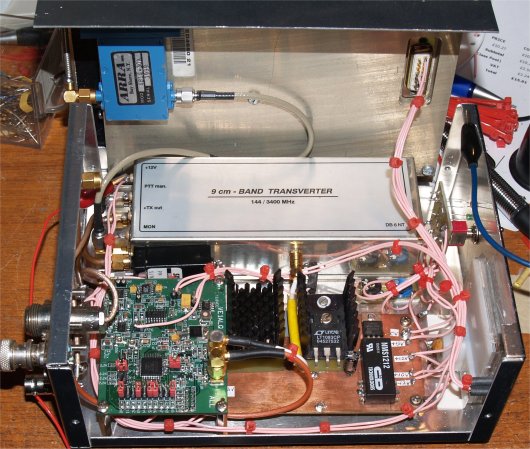
I started out on this, the final leg of the project, believing that I would be able to fit everything into one box only 205mm x 155mm x 75mm ... Hmmm?
I modified the transverter, configured the PLL board and tested it ... Yes! Sure, it’s going to fit! I told myself. But only just! I never throw out hardware, like nuts, bolts, washers ... metal pillars. I found four, only four, tapped metal pillars that just happened to be exactly the right height to mount the PLL board such that it straddles the PSU board, just clearing the electrolytic capacitor. With the two halves of the box put together there is little more than a millimetre between the PA and the two right-angled SMA connectors carrying the 10MHz reference and the 135MHz RF. I think it looks good.