Park Air Electronics 3010
23 minute read
This post is part of the series 'Park Air Electronics Series 3000':
Following on from my discussion of the PAE 3030 UHF Air-Band Transceiver, the following is an account of my experience whilst repairing a PAE 3010 VHF Transceiver.
It isn't unusual to receive these transceivers with the front panel in Remote configuration due to the fact that the operators in control of the AR-327 (T101) radar system are necessarily not actually 'on site'. There is always the possibility that the radar system be 'taken out' by an anti-radar missile, and should that occur, it is best that the operators are elsewhere. This particular transceiver arrived with the front panel in a peculiar state which necessitated a system reset. This is accomplished by holding in the red CE button whilst switching the transceiver on ... resulting in the frequency display reading 305.000 and the front panel defaulting to remote. There isn't actually a Remote indicator, rather the 'Local' LED to the right of the number 3 button will be unlit. This implies the panel is in non-local or Remote mode. Setting it to Local mode is accomplished by pressing the blue button then the number 3 button. This will cause the 'local' LED to illuminate.
Exactly why the frequency after 'reset' defaults to 305MHz is a bit of a puzzle since that is within the range of the PAE 3030. I suspect this might be because as far as I can ascertain, the firmware controlling the front panel is common to both the 3010 and the 3030 ... obviating the requirement to have different sets of firmware.
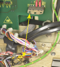 Left: Just on the off-chance that something was amiss behind the front panel, I removed the eight screws and folded it down. The wiring immediately behind the front panel is a tad cramped. I noticed that the 'fin' on the audio amplifier (IC36) exhibited signs of possible arching and that contact had been made with the DC Supply LED. However, in this case, since the fin is totally isolated, it is unlikely that arching was the cause. Checking the yellow wire to the DC supply LED: According to the circuit diagram for the main PSU, that particular wire should be violet. When it leaves the PSU board, it is violet … so why is it Yellow? Answer: It goes through two connectors on the BITE Assy. board before arriving at the LED ... Violet wire onto the BITE board … yellow wire on leaving the board. Why on earth change the colour of the wire?!! At least with the RA17 etc. you know where you are with wires … blue is the anode circuit, orange is the screen-grid and yellow is grid-1. In the end I concluded that the marks on the fin were simply corrosion. Then one of the pins on the LED broke off. Fortunately I had a spare in stock. I noticed that Links LK2 and LK3 were not fitted. These appear to set the Side Tone for 3030 or 1207 operation. I have no idea what a 1207 is. I fitted the two links in the 3030 position.
At this point, it was looking as if the transceiver was working ... but then it threw up a BITE error code of 5-4 in the Monitor Display. With BITE error codes, the first number is the Module number and the second number refers to the test that has failed. Module 5 is the Remote Control Decoder Module. However there is no mention of Module-5 error codes in the manual. Interestingly, waiting about 30 seconds after switching on, then running Interruptive BITE appeared to clear the fault. This sounded rather familiar … like the -10V line taking time to 'wind itself up' on a previous 3030. So, I decided to take the PSU board out and investigate things further. Getting the PSU board out is a tedious albeit not difficult job. See the three photographs below.
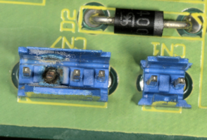
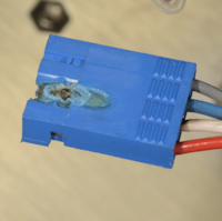
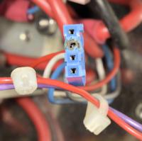
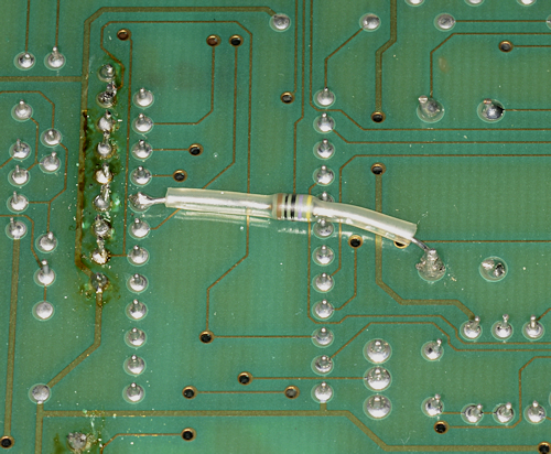
I did wonder why this little 4-pin header was reluctant to come away. Looks like pin 2 had disintegrated … part of the low-current +28V line which gets by-passed by a high-current relay on switch-on. All it takes is a bad connection to cause a voltage drop, and thus produce heat. This is what I think occurred here. I was able to order a replacement 4-pin connector to replace CN7 and a matching 4-pin free socket. While I waited for these to arrive, I put the PSU board on the bench and checked out all the voltage regulators, in particular the -10V rail.
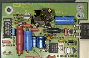
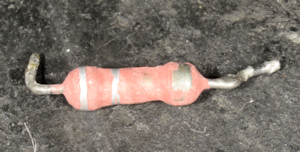
It is very likely that the 5-4 error code was a direct result of the burned out pin in CN7, however tests confirmed that the -10V line was a tad sluggish in reaching full potential. This is becoming a common occurrence in PAE series 3000 transceivers. The most common cause of this fault involves C7 and C9 on the output of the switching regulator exhibiting high ESR, typically 20 ohms. Other faults in this circuit have been an open circuit 6.2V Zener (D11) and a badly stressed 0R22 resistor (R6). In this case, C7 and C9 were both exhibiting high ESR, D11 measured 5.7V and R6, although measuring 0R22, was severely stressed.
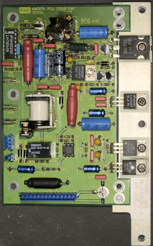
The photograph on the right shows the repaired PSU board. R6 was replaced with a 1.5W version. D11 was replaced with a new 1.3W 6.2V Zener and C7 and C9 were replaced. The board was re-tested on the bench and all supplies were verified as in-spec.
Next post in the series: Park Air Electronics Series 3000 Summing-Up ... with a Happy Ending
- Park Air Electronics 3030
- Park Air Electronics 3010
- Park Air Electronics Series 3000 Summing-Up ... with a Happy Ending
April 2026
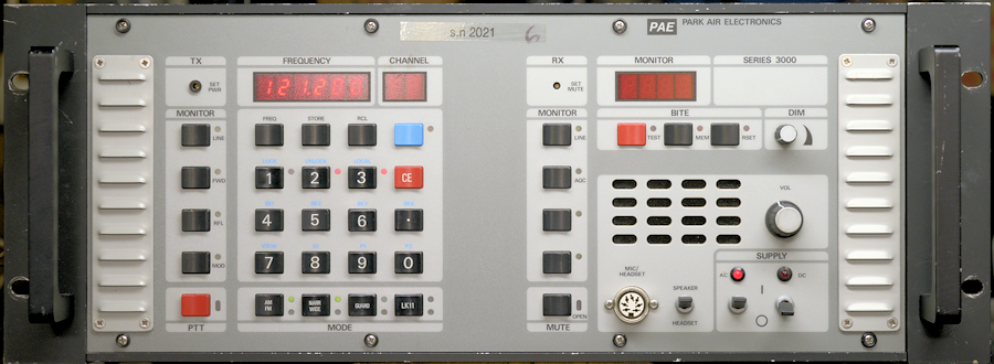
PAE 3010 Serial Number 2021.
Following on from my discussion of the PAE 3030 UHF Air-Band Transceiver, the following is an account of my experience whilst repairing a PAE 3010 VHF Transceiver.
It isn't unusual to receive these transceivers with the front panel in Remote configuration due to the fact that the operators in control of the AR-327 (T101) radar system are necessarily not actually 'on site'. There is always the possibility that the radar system be 'taken out' by an anti-radar missile, and should that occur, it is best that the operators are elsewhere. This particular transceiver arrived with the front panel in a peculiar state which necessitated a system reset. This is accomplished by holding in the red CE button whilst switching the transceiver on ... resulting in the frequency display reading 305.000 and the front panel defaulting to remote. There isn't actually a Remote indicator, rather the 'Local' LED to the right of the number 3 button will be unlit. This implies the panel is in non-local or Remote mode. Setting it to Local mode is accomplished by pressing the blue button then the number 3 button. This will cause the 'local' LED to illuminate.
Exactly why the frequency after 'reset' defaults to 305MHz is a bit of a puzzle since that is within the range of the PAE 3030. I suspect this might be because as far as I can ascertain, the firmware controlling the front panel is common to both the 3010 and the 3030 ... obviating the requirement to have different sets of firmware.
At this point, it was looking as if the transceiver was working ... but then it threw up a BITE error code of 5-4 in the Monitor Display. With BITE error codes, the first number is the Module number and the second number refers to the test that has failed. Module 5 is the Remote Control Decoder Module. However there is no mention of Module-5 error codes in the manual. Interestingly, waiting about 30 seconds after switching on, then running Interruptive BITE appeared to clear the fault. This sounded rather familiar … like the -10V line taking time to 'wind itself up' on a previous 3030. So, I decided to take the PSU board out and investigate things further. Getting the PSU board out is a tedious albeit not difficult job. See the three photographs below.
Burned out header pin.
Damaged free socket.
Damaged free socket.
I did wonder why this little 4-pin header was reluctant to come away. Looks like pin 2 had disintegrated … part of the low-current +28V line which gets by-passed by a high-current relay on switch-on. All it takes is a bad connection to cause a voltage drop, and thus produce heat. This is what I think occurred here. I was able to order a replacement 4-pin connector to replace CN7 and a matching 4-pin free socket. While I waited for these to arrive, I put the PSU board on the bench and checked out all the voltage regulators, in particular the -10V rail.
Area around switching regulator, R6 removed.
R6 showing signs of stress.
It is very likely that the 5-4 error code was a direct result of the burned out pin in CN7, however tests confirmed that the -10V line was a tad sluggish in reaching full potential. This is becoming a common occurrence in PAE series 3000 transceivers. The most common cause of this fault involves C7 and C9 on the output of the switching regulator exhibiting high ESR, typically 20 ohms. Other faults in this circuit have been an open circuit 6.2V Zener (D11) and a badly stressed 0R22 resistor (R6). In this case, C7 and C9 were both exhibiting high ESR, D11 measured 5.7V and R6, although measuring 0R22, was severely stressed.
The photograph on the right shows the repaired PSU board. R6 was replaced with a 1.5W version. D11 was replaced with a new 1.3W 6.2V Zener and C7 and C9 were replaced. The board was re-tested on the bench and all supplies were verified as in-spec.
Repaired PSU board.
Differences between the 3010 and the 3030:
Apart from the obvious difference, where the 3010 is a VHF transceiver covering 108MHz to 156MHz (actual 155.975MHz) and the 3030 is a UHF transceiver covering 225MHz to 400MHz (actual 399.975MHz), both models share the same Transmitter Control Module and BITE board. Whereas the RX module in the 3030 is limited to UHF only, the same module in the 3010 is dual-band. The reason for this is that the same RX module used in the 3010 and the 3050 which is a dual-band transceiver.
In the case of the 3010, the first IF is 250.7MHz, thus the local oscillator is the receive frequency + 250.7MHz (358.7MHz to 406.675MHz). In the case of the 3050, and where UHF is concerned, the first IF is 70.7MHz, in which case the synthesiser will provide a local oscillator of between 295MHz and 470.675MHz. The actual RF amplifier is a broadband stage common to both VHF and UHF receivers. Selection of the appropriate input preselector filter is controlled by the BITE control board behind the front panel. The output from the RF amplifier is fed to the 1st Mixer, the output of which is fed to the 1st IF amplifier and then on to either a 70.7MHz helical filter (UHF mode) or a 250.7MHz helical filter (VHF mode).
In the photograph above, the eight selectable preselector filters are on the left, sandwiched between PIN diode switches. Further to the right is the broadband RF amplifier, 1st Mixer and 1st IF amplifier stage. The two helical filters are on the far right. The 250.7MHz filter at the top with the larger 70.7MHz filter at the bottom with the selector circuitry in between. Admittedly this is a simplified description.
At first sight, the IF & AF Modules in the 3010 and 3030 look identical. However they have completely different drawing numbers of 68-30300012 and 68-38500008 respectively. The difference is to be found under the aluminium cover.
As with the 1st Local Oscillator, the 2nd LO is provided by the Synthesiser Module. However, the 2nd LO is derived from a fixed 60MHz signal. In the 3010 (and 3050 in VHF mode) this is multiplied by 4 to give 240MHz which when applied to the 2nd mixer is used to mix the 250.7MHz 1st IF down to 10.7MHz. In the 3030 (UHF) the 60MHz fundamental is used to mix the 70.7MHz 1st IF signal down to 10.7MHz.
A third Local Oscillator at 11.155MHz is used to further mix the signal down to a 3rd IF of 455KHz. There after, both the Wide-Band and Narrow-Band detection circuits are by and large very similar.
The above photograph shows the Synthesiser module with the cover removed. This module can be 'divided' into three operational parts. On the left is the control board based around an 8031 microcontroller. The other two parts are fairly typical of synthesisers of the day (1990s) and are actually not too dissimilar from that found in the Racal 1770 series from the 1970s, although the IC-count is understandably much lower. The section in the centre is the 7 selectable VCOs covering 100MHz to 471MHz. The section on the right is the dividers and PLLs. The Synthesiser module provides the 1st and 2nd Local Oscillator signals on receive and the Transmit frequency. When the mode of operation is FM, the modulation is applied within the synthesiser.
Although the synthesiser hardware appears common across the series, the firmware is peculiar to the type, and there is a degree of 'personalisation' as the EPROM on each synthesiser bears the serial number of that particular module.
I know, from the description in the manual, that when transmitting, a 'look up' table is used to provide for Direction Coupler Compensation. I don't know to what degree this compensation applies, but I do know that it is applied within the Loop Amplifier circuit on the BITE Assy., that controls the bias (and thus gain) of the driver stage in the RFPA. Since there is no mention in the manual of a look up table in the firmware on the BITE Assy., I have to conclude that the afore mentioned look up table is on the EPROM in the Synthesiser ... hence the module serial number on the EPROM label.
Above is the Transmitter Control Module in the 3000 series. I have come across two variations of this module. For a description of how these differ, see my earlier article on the 3030. This module provides the following: The Amplitude Modulation drive signal as well as TX audio compression in the form of RF-clipping, AM and FM modulation level control and control over the RF output from the PA. There is a control on the front panel for setting the RF output, but there is a further control on the TX Controller for setting the maximum FM power level independently.
It has to be said that the RF Power Amplifiers in the PAE 3000 series transceivers are beautifully made and extremely robust. There are two types of PA, VHF or UHF, both of which are designed to take the 100mW drive from the Synthesiser Module up to 40W of AM or 60W of FM. The VHF RFPA in the 3010 employs FETs throughout the gain path. This is formed from two self-contained modules, a driver stage and a PA stage. The driver stage consists of an MRF160 followed by an MRF136 driving an MRF171. The RFPA in the photographs above dates from 1998.
TR1 is described as an MRF160 and appears to be a TO-39 device. However, I have several Motorola RF data books from the early 1990s, none of which list the MRF160. A search of the internet yields many MRF160 datasheets, all of which show the device case as style 249-6, NOT TO-39. All such datasheets describe the MRF160 as a relatively high-gain FET (16dB) capable of 4W output, and specifically suitable for Class-A operation, thus ideal for linear operation. Motorola describe the MRF136 (TR2) as a 15W (o/p) device with a narrowband gain of 16dB and the MRF171 (TR3) as a 45W (o/p) device with a minimum gain of 12dB.
As with the UHF PA Driver, the VHF PA Driver acts as the Amplitude Modulator. This is accomplished via the Power and Modulation input which serves three purposes. When PTT is activated, the Power and Modulation input which is slightly -ve during receive, goes positive and biases TR3 on by way of TR4 and TR5. It also provides bias for TR1 and TR2. However, as the modulation signal is superimposed on this dc-level, this 'modulates' the gain of TR1 and TR2. The actual dc level applied is dictated by a look-up table in the Synthesiser EPROM and is intended to compensate for variation in Directional Coupler response.
When installed in a 3050, the Driver Stage in the VHF RFPA also serves as the common RF input on VHF and UHF. In this case, a built-in PIN-Diode switch controlled by a VHF/UHF Select line diverts the UHF signal from the Synthesiser over to the UHF PA ... a rather elegant feature. In the 3010, the PIN switch is permanently inoperative.
The Output stage employs a pair of MRF174s in parallel. With each device rated at 125W output, this stage is capable of safely delivering at least 200W, should it receive enough drive. Since the maximum output power of the PAE 3010 is given as 40W on AM or 60 on FM, none of the RF devices in the RFPA are likely running at more than 25% maximum ratings.
One part of the series 3000 transceivers that I have not yet discussed is the Power Regulator. This consists of two boards, one on top of the other, mounted on the left-hand heat sink. This is the module which delivers the +20V or +25V to the RFPA. Although the combined boards are referred to as the Power Regulator, and carry the drawing number 68-30300004, the silk-screen on the boards themselves identifies them as Power Modulator 1 and 2 respectively. I found this decidedly confusing at first, since looking at the circuit diagram, they are little more than three high current series regulators ... one for the RFPA Driver and one for each half of the output circuit. The main board delivers the current whilst the smaller 'daughter-board' looks after the regulation.
The last remaining board in the transceiver is the Remote Control Decoder which allows the transceiver to be controlled from a remote location. This is the only board in the transceiver that I am unable to test, for reasons which will become clear in my next article. This board is briefly described in my article on the PAE 3030.
Having satisfied myself that this particular 3010 was working, I connected it up to my HP8920. I confirmed that the receiver more than satisfied the manufacturer's specifications, and although Park Air only ask that the sensitivity is checked at 155.975MHz, I verified the sensitivity and noise figure at 108MHz also. The HP8920 was also used for setting up the AM and FM modulation levels, and then double checked using a Racal-Dana 9008, whilst a Bird Power Meter was used to measure the RF output INTO A DUMMY LOAD.
Although I was happy with the overall performance, a couple of things 'niggled' me. The transceiver has a built in monitor system whereby the 'Monitor' display on the right of the front panel can display the Modulation Level, Forward Power or Reflected Power. Whereas the Modulation level was almost 'spot on', the Forward Power reading was in in the order of 20% low. I knew that the output power was well within spec. having verified it on several different Bird Power Meters and different detector slugs. The problem here is that there is no mention in the manual on how to 'calibrate' the internal power monitor, nor is there any specific reference to this in the alignment section of the Technical Manual. The other thing that was nagging me was that although there is no Guard Receiver Installed, the associated button on the front panel and LEDs were active. The disparity with the internal power monitor could wait ... maybe I would figure out how to 'calibrate' that later. The fact that the 'ghost' Guard Receiver could be switch off and on was more pressing.
Initially I thought it was a firmware quirk, but that turned out not to be the case. Then after much poking around on the BITE board with an oscilloscope and getting nowhere, I hit on the idea of swapping boards with another transceiver. But herein was a problem ... the other two transceivers that I had in the workshop at the time were 3030s. I had already tried swapping the BITE board, and I was fairly certain that since this was a receiver issue, I could rule out the Transmitter Control board. Swapping the Synthesiser and Receiver boards was out of the question on account of the fact that this was a VHF transceiver and the 3030s are UHF transceivers. The Remote Control Decoder Modules in both 3030s were out of action for a reason which will be discussed in my next article. So that left the IF & AF Module. I swapped it out and BINGO! The LEDs for the Guard Receiver did not come on and the button was inactive. But why?
Since everything to do with the Front Panel is run by an 8031 microcontroller, it was logical, pun intended, to 'look' at the Data bus. But because everything is multiplexed, it is almost impossible to tell what is correct or incorrect. So I took the simple approach of measuring the resistance to +5V of the Data lines on the common bus ... i.e. on the 'outside' of the BITE board. The interface with the common Data bus for each module is an 8243 I/O Expander. Only the first 4 bits (0 - 3) are used in each case. I found that the resistance to +5V on the 'faulty' IF/AF module was significantly lower than on a 'working' one, and bit-0 was lower still. The first thing that I noticed was the the two pull-up resistor networks on the suspect board were 10K whilst the other board had 100K networks. A check in the Items list and ALL other modules revealed that 100K networks were specified. I didn't have any in stock, so I ordered a pack of ten. In the interim, I removed the 10K networks, and in order to do that, the board needs to come off its 'chassis' or back-plate. See the photographs below for what I discovered.
When you think about it, it is very obvious what has happened here. Whoever implemented this 'seemingly undocumented' modification, has counted along the pins of IC28, but on the wrong side. Thus Port-2 Bit-0 input (IC28 pin-8) has been taken to 0V via 47-ohms rather than the corresponding output of Port-6 (IC28 pin-16). Its an easy mistake to make, but how did it get past inspection? Was it EVER tested? I felt sure that this was the cause of the Guard Receiver button and LEDs being functional. I decided that since I was going to replace the 10K network resistors with the correct 100K type, it couldn't 'hurt' to temporarily fit discrete 100K resistors ... hence the evidence of rework and flux in the photograph. I moved the resistor from pin-8 over to pin-16 and was rewarded with a correctly functioning Front Panel where the Guard Receiver Button was now inoperative and the two LEDs remained OFF. The replacement 100K network resistors arrived a few days later, were subsequently fitted and the flux was duly cleared from the board.
I then returned to the issue with the built-in power monitor ... and I finally figured out how to calibrate it ... or at least the Forward Power part of it. Park Air are not joking when they describe the BITE Assembly board is a complex digital circuit which requires advanced fault finding techniques. Although what I think they are really trying to say is 'This board is very difficult to get your head around'. As its name suggests, it is the heart of the Built In Test Equipment or BITE. Yet, it controls the Front Panel and thus indirectly, the Synthesiser. It also controls the Transmitter output power, when you would expect that sort of thing to be within the remit of the Transmitter Control Module.
Writing this article has been very much a 'tell it to the duck' session, and as a result, I now have a greater understanding of how the Transmitter RF output is controlled. What muddies the water considerably is the fact that although the manual has a comprehensive section on how to set up the Transmitter Controller Module and in particular the part which controls the power output. The procedure in the manual pertaining to what they call the Analogue Multiplier is NOT relevant to Issue G modules. The procedure in the manual was written for Issue D modules where IC31 is a 16-pin MC1495. On the Issue G module, IC31 is an 8-pin AD633. Thus, the procedure in the manual makes reference to four trimmer potentiometers, while the later Issue G modules have only one.
I'm certain that changing IC31 was seen as a way of simplifying things. It's just a shame that the manual in my possession is out of date and Park Air are not able or willing to provide an update, citing that the equipment is obsolete and no longer supported.
It turns out that calibrating the Internal Forward Power Monitor is very simple. See the photograph on the left, with my trim tool pointing at the Forward Power adjustment potentiometer (actually labelled CAL on the schematic).
Note: The following is probably only valid if the transmitter and PA have been correctly aligned first. In which case, the SET PWR control on the Front Panel should NOT be fully clockwise for 40W of AM i.e. always 'give yourself some room'. Verify that the output is 40W. Select FWD on the MONITOR pane. The FWD LED should illuminate and a zero should appear in the MONITOR display. Press PTT. In my case, the MONITOR display was 34. Adjust the Calibration pot in the photograph above clockwise. The Power on the external power meter should drop, but the figure in the MONITOR display should remain static. Adjust the Calibration pot so that the External Power Meter reads the same as the Monitor display. Now adjust SET PWR for 40W on the External Power Meter. The MONITOR display should now read 40. Verify that there is also correlation of power measurement for 60W on FM. RV9 on the Transmitter Controller Module might need to be adjusted if the power on FM is too high or too low. However I found that RV9 did not require readjustment.
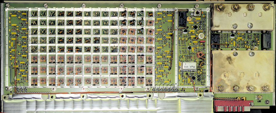
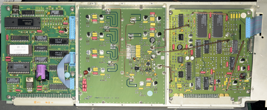
Apart from the obvious difference, where the 3010 is a VHF transceiver covering 108MHz to 156MHz (actual 155.975MHz) and the 3030 is a UHF transceiver covering 225MHz to 400MHz (actual 399.975MHz), both models share the same Transmitter Control Module and BITE board. Whereas the RX module in the 3030 is limited to UHF only, the same module in the 3010 is dual-band. The reason for this is that the same RX module used in the 3010 and the 3050 which is a dual-band transceiver.
RX Module as fitted in PAE 3010 and 3050.
In the case of the 3010, the first IF is 250.7MHz, thus the local oscillator is the receive frequency + 250.7MHz (358.7MHz to 406.675MHz). In the case of the 3050, and where UHF is concerned, the first IF is 70.7MHz, in which case the synthesiser will provide a local oscillator of between 295MHz and 470.675MHz. The actual RF amplifier is a broadband stage common to both VHF and UHF receivers. Selection of the appropriate input preselector filter is controlled by the BITE control board behind the front panel. The output from the RF amplifier is fed to the 1st Mixer, the output of which is fed to the 1st IF amplifier and then on to either a 70.7MHz helical filter (UHF mode) or a 250.7MHz helical filter (VHF mode).
In the photograph above, the eight selectable preselector filters are on the left, sandwiched between PIN diode switches. Further to the right is the broadband RF amplifier, 1st Mixer and 1st IF amplifier stage. The two helical filters are on the far right. The 250.7MHz filter at the top with the larger 70.7MHz filter at the bottom with the selector circuitry in between. Admittedly this is a simplified description.
IF and AF Module as fitted in PAE 3010 and 3050.
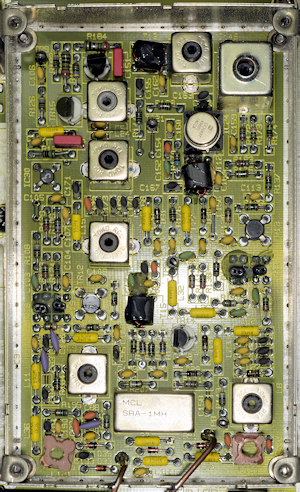
3010/3050 IF & AF Module 2nd Local Osc.
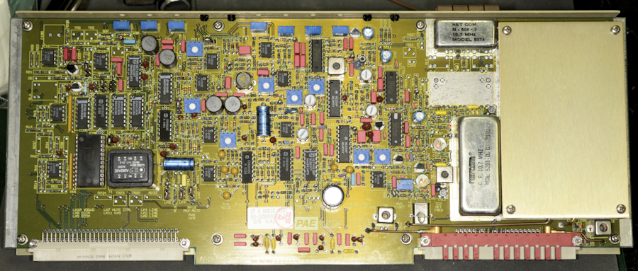
At first sight, the IF & AF Modules in the 3010 and 3030 look identical. However they have completely different drawing numbers of 68-30300012 and 68-38500008 respectively. The difference is to be found under the aluminium cover.
As with the 1st Local Oscillator, the 2nd LO is provided by the Synthesiser Module. However, the 2nd LO is derived from a fixed 60MHz signal. In the 3010 (and 3050 in VHF mode) this is multiplied by 4 to give 240MHz which when applied to the 2nd mixer is used to mix the 250.7MHz 1st IF down to 10.7MHz. In the 3030 (UHF) the 60MHz fundamental is used to mix the 70.7MHz 1st IF signal down to 10.7MHz.
A third Local Oscillator at 11.155MHz is used to further mix the signal down to a 3rd IF of 455KHz. There after, both the Wide-Band and Narrow-Band detection circuits are by and large very similar.
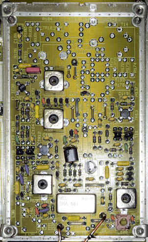
3030 IF & AF Module 2nd Local Osc.
Synthesiser Module common to all series 3000 transceivers (cover removed).
The above photograph shows the Synthesiser module with the cover removed. This module can be 'divided' into three operational parts. On the left is the control board based around an 8031 microcontroller. The other two parts are fairly typical of synthesisers of the day (1990s) and are actually not too dissimilar from that found in the Racal 1770 series from the 1970s, although the IC-count is understandably much lower. The section in the centre is the 7 selectable VCOs covering 100MHz to 471MHz. The section on the right is the dividers and PLLs. The Synthesiser module provides the 1st and 2nd Local Oscillator signals on receive and the Transmit frequency. When the mode of operation is FM, the modulation is applied within the synthesiser.
Although the synthesiser hardware appears common across the series, the firmware is peculiar to the type, and there is a degree of 'personalisation' as the EPROM on each synthesiser bears the serial number of that particular module.
I know, from the description in the manual, that when transmitting, a 'look up' table is used to provide for Direction Coupler Compensation. I don't know to what degree this compensation applies, but I do know that it is applied within the Loop Amplifier circuit on the BITE Assy., that controls the bias (and thus gain) of the driver stage in the RFPA. Since there is no mention in the manual of a look up table in the firmware on the BITE Assy., I have to conclude that the afore mentioned look up table is on the EPROM in the Synthesiser ... hence the module serial number on the EPROM label.
Transmitter Control Module, issue G.
Above is the Transmitter Control Module in the 3000 series. I have come across two variations of this module. For a description of how these differ, see my earlier article on the 3030. This module provides the following: The Amplitude Modulation drive signal as well as TX audio compression in the form of RF-clipping, AM and FM modulation level control and control over the RF output from the PA. There is a control on the front panel for setting the RF output, but there is a further control on the TX Controller for setting the maximum FM power level independently.
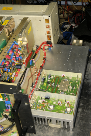
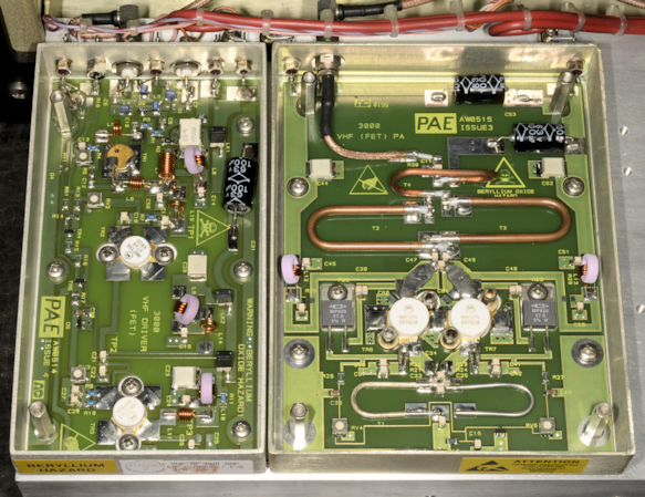
3010 RFPA hinged down for access.
3010 RFPA in detail.
It has to be said that the RF Power Amplifiers in the PAE 3000 series transceivers are beautifully made and extremely robust. There are two types of PA, VHF or UHF, both of which are designed to take the 100mW drive from the Synthesiser Module up to 40W of AM or 60W of FM. The VHF RFPA in the 3010 employs FETs throughout the gain path. This is formed from two self-contained modules, a driver stage and a PA stage. The driver stage consists of an MRF160 followed by an MRF136 driving an MRF171. The RFPA in the photographs above dates from 1998.
TR1 is described as an MRF160 and appears to be a TO-39 device. However, I have several Motorola RF data books from the early 1990s, none of which list the MRF160. A search of the internet yields many MRF160 datasheets, all of which show the device case as style 249-6, NOT TO-39. All such datasheets describe the MRF160 as a relatively high-gain FET (16dB) capable of 4W output, and specifically suitable for Class-A operation, thus ideal for linear operation. Motorola describe the MRF136 (TR2) as a 15W (o/p) device with a narrowband gain of 16dB and the MRF171 (TR3) as a 45W (o/p) device with a minimum gain of 12dB.
As with the UHF PA Driver, the VHF PA Driver acts as the Amplitude Modulator. This is accomplished via the Power and Modulation input which serves three purposes. When PTT is activated, the Power and Modulation input which is slightly -ve during receive, goes positive and biases TR3 on by way of TR4 and TR5. It also provides bias for TR1 and TR2. However, as the modulation signal is superimposed on this dc-level, this 'modulates' the gain of TR1 and TR2. The actual dc level applied is dictated by a look-up table in the Synthesiser EPROM and is intended to compensate for variation in Directional Coupler response.
When installed in a 3050, the Driver Stage in the VHF RFPA also serves as the common RF input on VHF and UHF. In this case, a built-in PIN-Diode switch controlled by a VHF/UHF Select line diverts the UHF signal from the Synthesiser over to the UHF PA ... a rather elegant feature. In the 3010, the PIN switch is permanently inoperative.
The Output stage employs a pair of MRF174s in parallel. With each device rated at 125W output, this stage is capable of safely delivering at least 200W, should it receive enough drive. Since the maximum output power of the PAE 3010 is given as 40W on AM or 60 on FM, none of the RF devices in the RFPA are likely running at more than 25% maximum ratings.
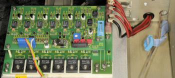
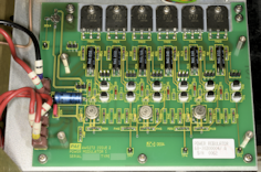
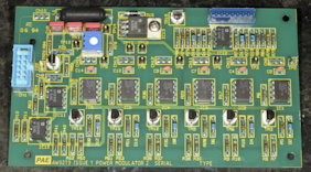
PA Regulator Assembly folded down.
PA Regulator Main Board.
PA Regulator Daughter Board.
One part of the series 3000 transceivers that I have not yet discussed is the Power Regulator. This consists of two boards, one on top of the other, mounted on the left-hand heat sink. This is the module which delivers the +20V or +25V to the RFPA. Although the combined boards are referred to as the Power Regulator, and carry the drawing number 68-30300004, the silk-screen on the boards themselves identifies them as Power Modulator 1 and 2 respectively. I found this decidedly confusing at first, since looking at the circuit diagram, they are little more than three high current series regulators ... one for the RFPA Driver and one for each half of the output circuit. The main board delivers the current whilst the smaller 'daughter-board' looks after the regulation.
The last remaining board in the transceiver is the Remote Control Decoder which allows the transceiver to be controlled from a remote location. This is the only board in the transceiver that I am unable to test, for reasons which will become clear in my next article. This board is briefly described in my article on the PAE 3030.
Having satisfied myself that this particular 3010 was working, I connected it up to my HP8920. I confirmed that the receiver more than satisfied the manufacturer's specifications, and although Park Air only ask that the sensitivity is checked at 155.975MHz, I verified the sensitivity and noise figure at 108MHz also. The HP8920 was also used for setting up the AM and FM modulation levels, and then double checked using a Racal-Dana 9008, whilst a Bird Power Meter was used to measure the RF output INTO A DUMMY LOAD.
Although I was happy with the overall performance, a couple of things 'niggled' me. The transceiver has a built in monitor system whereby the 'Monitor' display on the right of the front panel can display the Modulation Level, Forward Power or Reflected Power. Whereas the Modulation level was almost 'spot on', the Forward Power reading was in in the order of 20% low. I knew that the output power was well within spec. having verified it on several different Bird Power Meters and different detector slugs. The problem here is that there is no mention in the manual on how to 'calibrate' the internal power monitor, nor is there any specific reference to this in the alignment section of the Technical Manual. The other thing that was nagging me was that although there is no Guard Receiver Installed, the associated button on the front panel and LEDs were active. The disparity with the internal power monitor could wait ... maybe I would figure out how to 'calibrate' that later. The fact that the 'ghost' Guard Receiver could be switch off and on was more pressing.
Initially I thought it was a firmware quirk, but that turned out not to be the case. Then after much poking around on the BITE board with an oscilloscope and getting nowhere, I hit on the idea of swapping boards with another transceiver. But herein was a problem ... the other two transceivers that I had in the workshop at the time were 3030s. I had already tried swapping the BITE board, and I was fairly certain that since this was a receiver issue, I could rule out the Transmitter Control board. Swapping the Synthesiser and Receiver boards was out of the question on account of the fact that this was a VHF transceiver and the 3030s are UHF transceivers. The Remote Control Decoder Modules in both 3030s were out of action for a reason which will be discussed in my next article. So that left the IF & AF Module. I swapped it out and BINGO! The LEDs for the Guard Receiver did not come on and the button was inactive. But why?
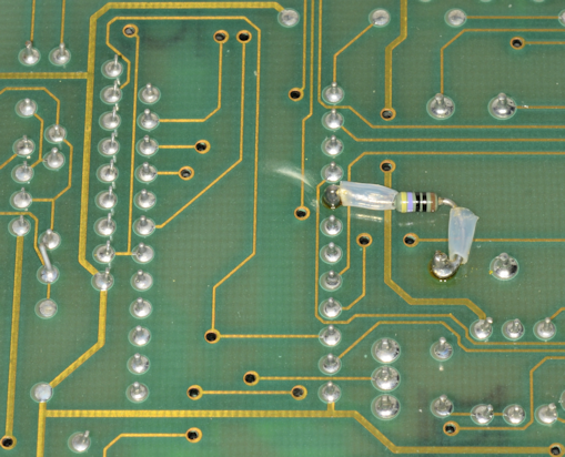
Since everything to do with the Front Panel is run by an 8031 microcontroller, it was logical, pun intended, to 'look' at the Data bus. But because everything is multiplexed, it is almost impossible to tell what is correct or incorrect. So I took the simple approach of measuring the resistance to +5V of the Data lines on the common bus ... i.e. on the 'outside' of the BITE board. The interface with the common Data bus for each module is an 8243 I/O Expander. Only the first 4 bits (0 - 3) are used in each case. I found that the resistance to +5V on the 'faulty' IF/AF module was significantly lower than on a 'working' one, and bit-0 was lower still. The first thing that I noticed was the the two pull-up resistor networks on the suspect board were 10K whilst the other board had 100K networks. A check in the Items list and ALL other modules revealed that 100K networks were specified. I didn't have any in stock, so I ordered a pack of ten. In the interim, I removed the 10K networks, and in order to do that, the board needs to come off its 'chassis' or back-plate. See the photographs below for what I discovered.
47R resistor in correct place.
WOOPS! 47R resistor in wrong place.
When you think about it, it is very obvious what has happened here. Whoever implemented this 'seemingly undocumented' modification, has counted along the pins of IC28, but on the wrong side. Thus Port-2 Bit-0 input (IC28 pin-8) has been taken to 0V via 47-ohms rather than the corresponding output of Port-6 (IC28 pin-16). Its an easy mistake to make, but how did it get past inspection? Was it EVER tested? I felt sure that this was the cause of the Guard Receiver button and LEDs being functional. I decided that since I was going to replace the 10K network resistors with the correct 100K type, it couldn't 'hurt' to temporarily fit discrete 100K resistors ... hence the evidence of rework and flux in the photograph. I moved the resistor from pin-8 over to pin-16 and was rewarded with a correctly functioning Front Panel where the Guard Receiver Button was now inoperative and the two LEDs remained OFF. The replacement 100K network resistors arrived a few days later, were subsequently fitted and the flux was duly cleared from the board.
Forward Power Calibration pot on VHF Directional Coupler.
I then returned to the issue with the built-in power monitor ... and I finally figured out how to calibrate it ... or at least the Forward Power part of it. Park Air are not joking when they describe the BITE Assembly board is a complex digital circuit which requires advanced fault finding techniques. Although what I think they are really trying to say is 'This board is very difficult to get your head around'. As its name suggests, it is the heart of the Built In Test Equipment or BITE. Yet, it controls the Front Panel and thus indirectly, the Synthesiser. It also controls the Transmitter output power, when you would expect that sort of thing to be within the remit of the Transmitter Control Module.
Writing this article has been very much a 'tell it to the duck' session, and as a result, I now have a greater understanding of how the Transmitter RF output is controlled. What muddies the water considerably is the fact that although the manual has a comprehensive section on how to set up the Transmitter Controller Module and in particular the part which controls the power output. The procedure in the manual pertaining to what they call the Analogue Multiplier is NOT relevant to Issue G modules. The procedure in the manual was written for Issue D modules where IC31 is a 16-pin MC1495. On the Issue G module, IC31 is an 8-pin AD633. Thus, the procedure in the manual makes reference to four trimmer potentiometers, while the later Issue G modules have only one.
I'm certain that changing IC31 was seen as a way of simplifying things. It's just a shame that the manual in my possession is out of date and Park Air are not able or willing to provide an update, citing that the equipment is obsolete and no longer supported.
It turns out that calibrating the Internal Forward Power Monitor is very simple. See the photograph on the left, with my trim tool pointing at the Forward Power adjustment potentiometer (actually labelled CAL on the schematic).
Note: The following is probably only valid if the transmitter and PA have been correctly aligned first. In which case, the SET PWR control on the Front Panel should NOT be fully clockwise for 40W of AM i.e. always 'give yourself some room'. Verify that the output is 40W. Select FWD on the MONITOR pane. The FWD LED should illuminate and a zero should appear in the MONITOR display. Press PTT. In my case, the MONITOR display was 34. Adjust the Calibration pot in the photograph above clockwise. The Power on the external power meter should drop, but the figure in the MONITOR display should remain static. Adjust the Calibration pot so that the External Power Meter reads the same as the Monitor display. Now adjust SET PWR for 40W on the External Power Meter. The MONITOR display should now read 40. Verify that there is also correlation of power measurement for 60W on FM. RV9 on the Transmitter Controller Module might need to be adjusted if the power on FM is too high or too low. However I found that RV9 did not require readjustment.
Next post in the series: Park Air Electronics Series 3000 Summing-Up ... with a Happy Ending