HP8591E repair
10 minute read
July 2026
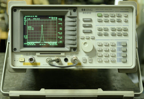
HP8591E
This compact little spectrum analyser was bought at auction for £50 and apparently worked rather well. However, recently it simply stopped working. No smoke or nasty surprises. It simply wouldn't switch on. "Would you be up to having a look at it? I think its probably just the switch-mode-PSU that's gone." ... said the owner.
So it arrived in a very solid wooden crate back in mid-May. I have to admit that I was surprised just how light it was, given that it is the same shape and size as my HP8920A ... and that is very heavy indeed.
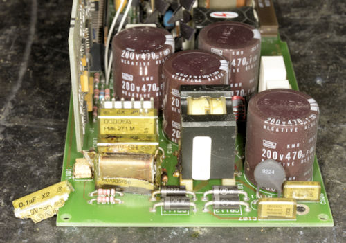
Exploded Rifa capacitors.
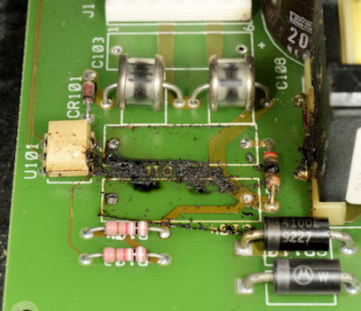
Explosion debris.
There is something satisfying about discovering a fault that you know you can fix. However, sometimes what appears to be the fault, and it can be quite obvious, may not be the actual fault … as I was to find out. It has to be said that Hewlett-Packard loved Rifa capacitors. I remember more than one occasion when I worked at Racal, when I picked up an item of HP test equipment and the Rifa capacitor across the mains discharged itself into a finger or thumb that came in contact with the IEC mains connector. Happy days! The blown resistor in the photograph on the right is in series with the exploded capacitor, across the mains input. I replaced ALL the Rifa capacitors (all had cracks) and U101, the opto-isolator. There was always the chance that this would bring the analyser back to life, but I was not surprised when it still would not power up.
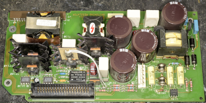 Repaired Switching-Regulator board.
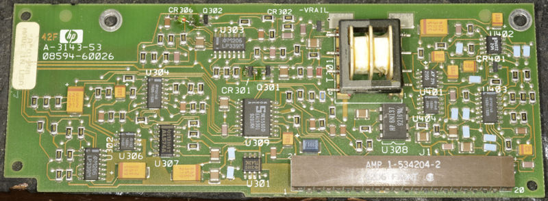 SMPS Controller board.
There are three boards that make up the SMPSU.This (above) is the Controller board, and U309 in the centre is the chip which controls everything. It looks like Hewlett Packard changed the way that power supplies were switched on when they introduced the 8590 series of analysers. Previously the mains switch was integral to the PSU and was operated by way of a long and sometimes oddly shaped plastic rod or bar which was attached to a button on the front panel. This arrangement worked, but was a devil to remove without breaking something.
While trawling the internet for clues as to why the oscillator might not be running, I found the answer on the HP-Agilent-Keysight Google.io group. Here I learned that this SMPS was powered as long as it was connected to the mains supply and the oscillator was only enabled when the front panel ‘Line’ switch was depressed. There are two Schottky diodes (CR301 and CR306) which are part of this ‘mechanism’ and if either of these fails, the oscillator will fail to start. That was what was wrong with this power supply. CR306 had gone ‘soft’, its forward voltage drop was less than 0.3V. I replaced it with a tiny non-smd Schottky diode, reassembled the SMPS and re-installed it.
On pressing the ‘Line’ button on the front panel, the PSU switched on but there was still a fault somewhere. On the top of the SMPS module there is a bank of LEDs which provide a quick indication regards the state of the various supply rails. In this case both the -15V and -24V LEDs were out. Note, the -24V line is only used if a particular hardware option is fitted, which in this case, it isn’t.
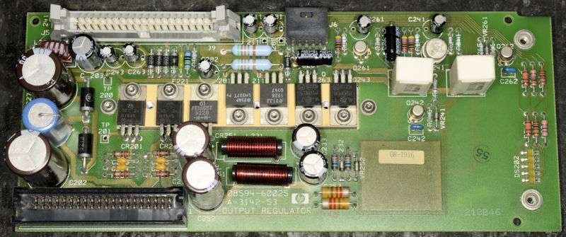 Output Regulator board.
The bank of LEDs (DS202) can be seen bottom-right in the above photograph. The reason for the ‘failed’ -15V rail was a short-circuit Tantalum bead capacitor on the Analog Interface board. I replaced ALL the three-legged tants on this board with aluminium types. This appeared to resolve the problem, but the analyser appeared about 20dB deaf … and the -24V LED was seen to come on then go out. Eventually it didn’t illuminate at all. This turned out to be nothing more than a faulty LED.
Fortunately I had an identical diode at hand. I snipped the faulty one from the array and fitted the replacement. All LEDs now illuminated but the analyser was definitely deaf.
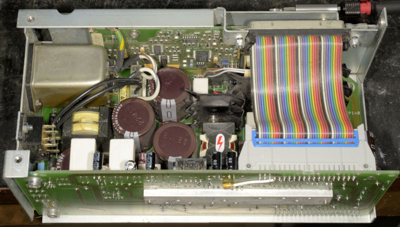 SMPS, cover removed (prior to replacing CR306).
As well as the apparent deafness, I noticed that the bottom left corner of the display looked ‘smudged or out of focus. I managed to remove the entire RF Front-End assembly. The idea was to investigate the deafness. I figured a faulty input attenuator or first mixer. Identifying the attenuator was easy, as was the first mixer. The attenuator was removed, tested on the bench and found to be not faulty … all sections functional. The mixer assembly was examined and looked immaculate. Both diodes appeared to be ‘good’.
While the front end was out of the chassis, I took the opportunity to clean the front of the display tube. An accumulation of dust being the cause of the ‘obscured’ corner of the display. Having cleaned the front of the CRT, I carefully re-fitted the RF Front-End assembly and Front Panel.
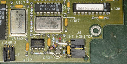
Monitor connector
At this point the display suddenly became unreadable. The signals to the display originate from a 5-pin connector on the corner of the main Processor Board (see left). Both the Horizontal and Vertical Sync signals appeared to be incorrect … the period between the pulses being almost but not exactly twice what they should be. This kind of fault is mentioned in the service manual, but the solution is not very helpful as it tells you to re-load the display factory-defaults. But to do that, one has to be able to navigate the menu on the display … which was unreadable.
However, with some subtle tweaking of the display controls, I was able to achieve a display that was moderately readable, although there was clearly some horizontal and vertical wrapping. This enabled me to then re-load the default settings for the display, and after re-tweaking the horizontal and vertical sync controls on the display, I managed to restore the display.
Clearly something had corrupted the stored settings, or maybe they had been completely lost. Either way, I decided to ‘look’ at the battery back-up circuit.
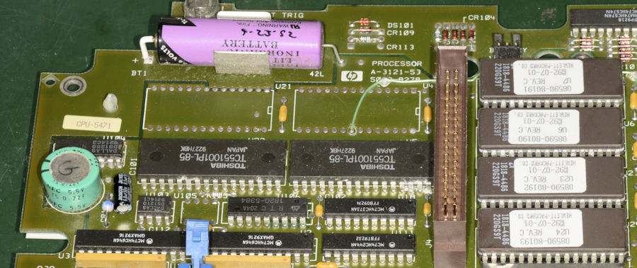 Battery, Super-Cap and RAM etc.
The Supercap is on the left. To the right of it is a Schottky diode which I discovered was failing. Its forward drop was only 0.15V when the spec was 0.6V. I replaced it with another Schottky diode with a forward drop of 0.6V. I also replaced the adjacent tant with an aluminium type. At the top of the above photograph is an enigma. The Lithium battery was at least 10 years old and still reading 3.6V. I ordered a replacement anyway. To the right of the battery are two diodes. DS101 is an axial LED and CR109 is probably a 1N4148. These are in series and connected across the battery. WHY? What is even stranger is the fact that in their current configuration the LED will never illuminate, unless the battery is reversed. If the two diodes are reversed, the LED will illuminate, but that would ultimately exhaust the battery prematurely, which simply doesn’t make sense. So I have to conclude that in their current configuration, which according to the cct diag., is correct, is HP’s way of letting you know that you have just connected the battery the wrong way round … although there is NOTHING in the manual about this.
Something else that I had noticed was an inconsistency in the analyser’s level of deafness. This was either 20dB or 10dB and appeared to be linked to whether Amplitude Cal had been initiated. This I concluded, suggested that the stored calibration data was either corrupt or in need of updating. Running Amplitude Cal threw up a whole raft of bandwidth shape errors which suggested that one or both of the Crystal and LC Bandwidth Filter boards (A11 and A13) were out of alignment.
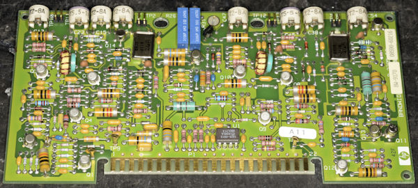
08590-60216
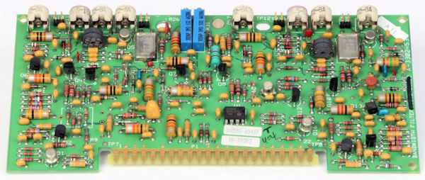
08590-60407 (example of)
Examining the two boards (which are identical) the first thing I noticed was that both were labelled as A11. This suggested that the one in position A13 was a replacement, or both were.
The second thing that came to light was that the one in position A13 did not appear to be functioning correctly. See below
The third thing that came to light was that these boards (drg. No. 08590-60216) did not appear to be intended for the 8591E. According to official documentation, the correct boards should be 08590-60407.
Whilst two correct boards were ordered, I discovered that it was the board in position A11 that was actually faulty. I found a broken track on the back. Once repaired, I was able to perform an alignment of both boards.
As can be discerned from the two photographs on the left, the boards differ significantly, with one having TO-18 transistors whilst the other is predominantly TO-92 types. The layout is also different and the schematics for each board confirm this. As I said, I did manage to perform a full calibration, but as soon as I pressed Store, the display corrupted. Clearly something corrupted the data. Maybe storing new data ‘on top of’ old data caused an anomaly.
Fortunately I was able to ‘Clear’ the old Cal Data by using a password-protected procedure and store the new data. I have not been able to replicate the anomaly.
When the new (correct) boards arrived, the 60216s were replaced with 60407s. I had to go through the alignment procedure three times until all bandwidth filter shape errors were eliminated and the the subsequent calibration data was stored to memory.
Worth noting here ... the calibration procedure in the Service Manual is incorrect ... it appears to 'skip' several key adjustments. I found the following corrected procedure on EEVBlog ...
25. Short A11TP10-11, A11TP12-13, and A13TP10-11 using the crystal shorts used in the crystal alignment section. Press the following analyzer keys -
BW, 30, kHz
SPAN, 200, kHz
MKR FCTN, MK TRACK ON OFF (OFF)
BW, 100, kHz
26. Adjust A13C45 (A13 - 2nd LC) for maximum signal at center-screen.
27. Move the short from A13TP10-11 to A13TP12-13, then adjust A13C23 (A13- 1st LC) for maximum signal at center-screen.
28. Move the short from A11P12-13 to A13P10-11, then adjust A11C45 (A11- 2nd LC) for maximum signal at center-screen.
29. Move the short from A11TP10-11 to A11TP12-13, then adjust A11C23 (A11- 1st LC) for maximum signal at center-screen.
BW, 30, kHz
SPAN, 200, kHz
MKR FCTN, MK TRACK ON OFF (OFF)
BW, 100, kHz
26. Adjust A13C45 (A13 - 2nd LC) for maximum signal at center-screen.
27. Move the short from A13TP10-11 to A13TP12-13, then adjust A13C23 (A13- 1st LC) for maximum signal at center-screen.
28. Move the short from A11P12-13 to A13P10-11, then adjust A11C45 (A11- 2nd LC) for maximum signal at center-screen.
29. Move the short from A11TP10-11 to A11TP12-13, then adjust A11C23 (A11- 1st LC) for maximum signal at center-screen.
Also: The Crystal Shorts that the procedure refers to are simply a 90R resistor (2 x 180R in parallel) in series with 10nF.